Logisim CPU
24-cycle Y86-style processor built in Logisim
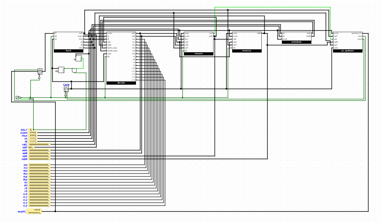
This project was part of my Computer Organization (CSCE312) class: a CPU built in Logisim with a staged datapath for a Y86-style instruction set. The design breaks each instruction into the same familiar values used in the architecture labs: icode, ifun, rA, rB, valC, valP, valA, valB, valE, and valM.
The interesting part was making the whole processor run predictably in hardware logic. Instead of allowing each instruction to take a different path length, the main circuit uses a cycle counter to normalize execution to 24 clock cycles per instruction:
- cycles
0-9: fetch the 10-byte instruction from ROM - cycle
10: decode and read the register file - cycle
11: execute the ALU operation and update condition codes when needed - cycles
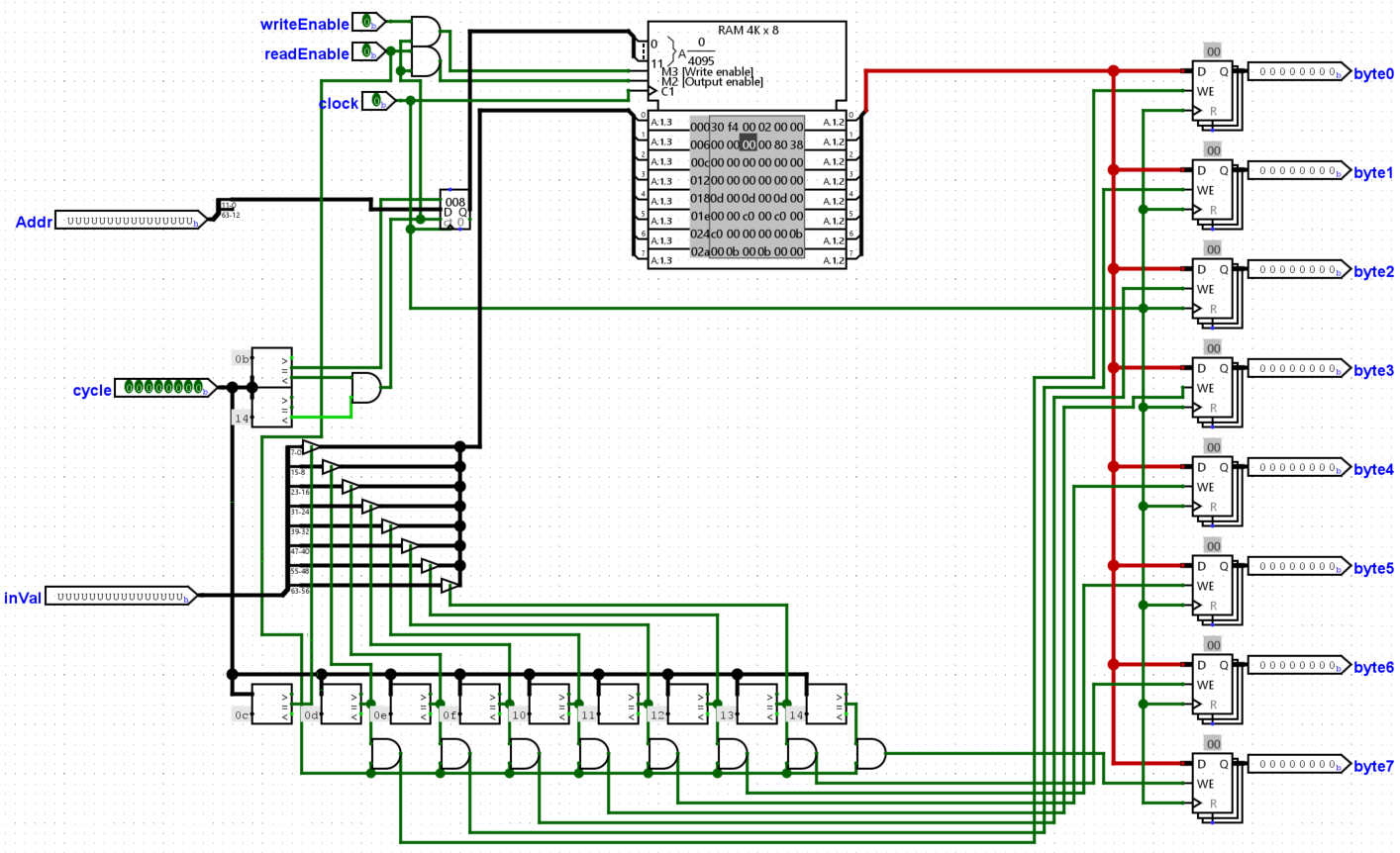
12-20: read from or write to RAM - cycle
21: write results back to the register file - cycles
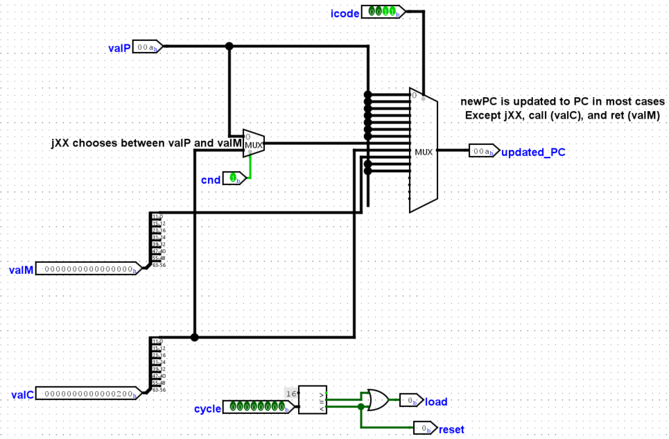
22-23: update the program counter and reset the cycle counter
Architecture
The processor is split into the usual stages:
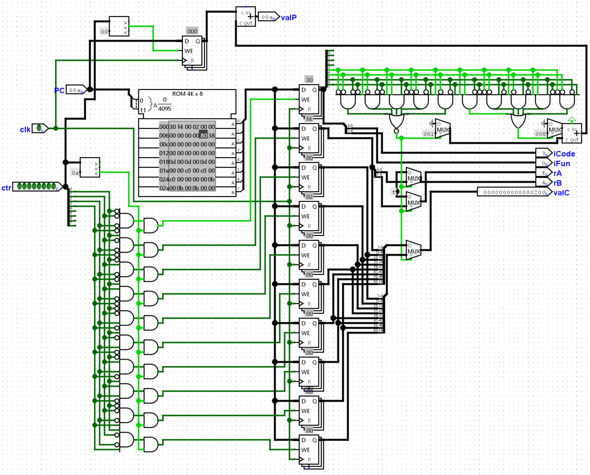
- Fetch reads a 10-byte instruction from ROM, extracts the instruction fields, and calculates
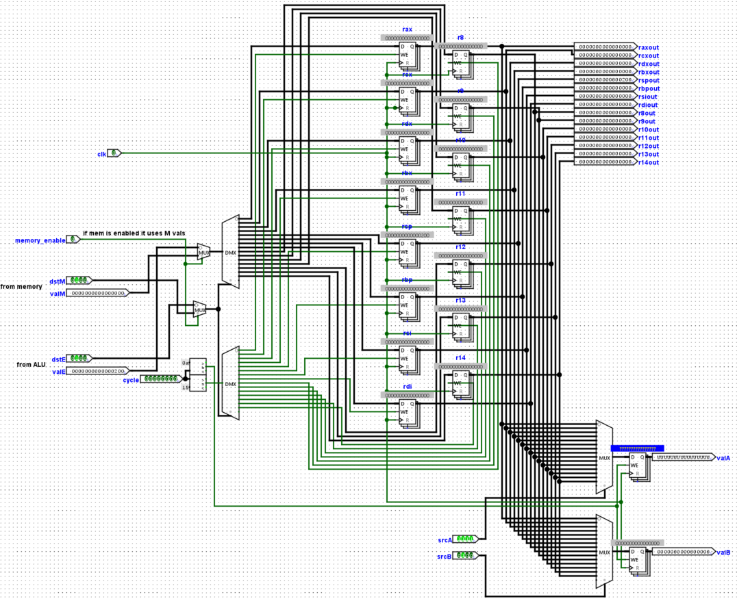
valP. - Decode selects
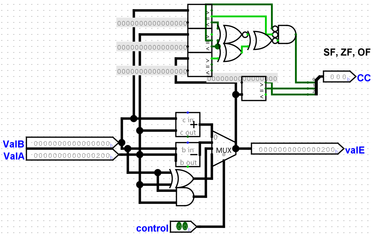
srcAandsrcB, readsvalAandvalBfrom the register file, and supports write-back throughdstE,dstM,valE, andvalM. - Execute uses ALU input selectors for
aluAandaluB, decodesifunfor arithmetic/logical operations, and setsZF,SF, andOFcondition codes. - Memory controls RAM reads and writes through address/data muxes and enable logic.
- Write-back decides whether results should be written from the ALU or memory path.
- PC update chooses the next PC from
valP,valC, orvalM, depending on calls, returns, and conditional control flow.
Takeaway
This project made the abstract CPU diagrams from class feel much more real. Wiring the datapath by hand forced me to think about control signals, mux selection, register timing, memory latency, and how much hidden sequencing is behind a single assembly instruction.